NanoWorldMaps
NanoWorldMaps will become Europe’s distributed Research Infrastructure for Ultra-Fast 2D/3D Imaging in life and material sciences
NanoWorldMaps
NanoWorldMaps will become Europe’s distributed Research Infrastructure for Ultra-Fast 2D/3D Imaging in life and material sciences
Ultra-Fast and Extra-Large Area 2D/3D Imaging
NanoWorldMaps works on empowering Europe to lead the revolution in high-throughput multimodal imaging at the nanometre scale. NanoWorldMaps will become a distributed European Research Infrastructure to provide cutting-edge enabling technologies as a service:
NanoWorldMaps services will be focused on the needs of scientists from academia and industry in a growing list of strategic application areas:
Ultra-Fast and Extra-Large Area 2D/3D Imaging for material and life scientists
NanoWorldMaps works on empowering Europe to lead the revolution in high-throughput multimodal imaging at the nanometre scale. NanoWorldMaps will become a distributed European Research Infrastructure to provide cutting-edge enabling technologies as a service:
NanoWorldMaps services will be focused on the needs of scientists from academia and industry in a growing list of strategic application areas:
Connectomics
Analysis of the connections of nerve cells by scanning and stacking thin sections of entire brain areas or brains at nanometre scale.
Battery research
Scanning of whole battery electrodes at nanometre scale. Development of battery cell components and production research.
Microelectronics
High-throughput multimodal imaging at nanometre scale for next-gen chip and microelectronics development.
Nanostructures
High-throughput nanometre scanning for the development of nano-machines, nano-structured components and 2D materials.
NanoWorldMaps Services
NanoWorldMaps enables researchers from academia and industry to use cutting-edge Ultra-Fast Large Area 2D/3D Imaging technologies in three different formats. NanoWorldMaps is currently in the concept phase and is working on an integrated service delivery concept from sample preparation and image acquisition to data evaluation using supercomputers and Artificial Intelligence and the provision of validated data on different science cloud systems.
Access Program
Develop new methods or work on your scientific questions. Use the future NanoWorldMaps Access Program as an assisted and funded access to the infrastructure.
Beamtime Booking
Use the future NanoWorldMaps workflows for your scientific questions and simply book beam time according to your needs.
Multi-Node Projects
Scientists with very high imaging requirements can use the Multi-Node Project service of combining the imaging power of several future NanoWorldMaps nodes.
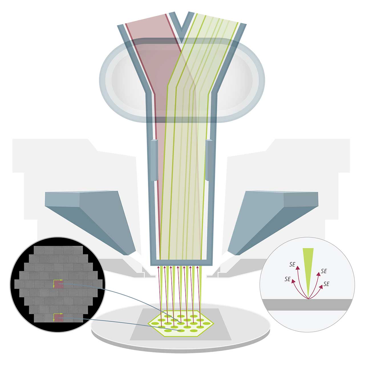
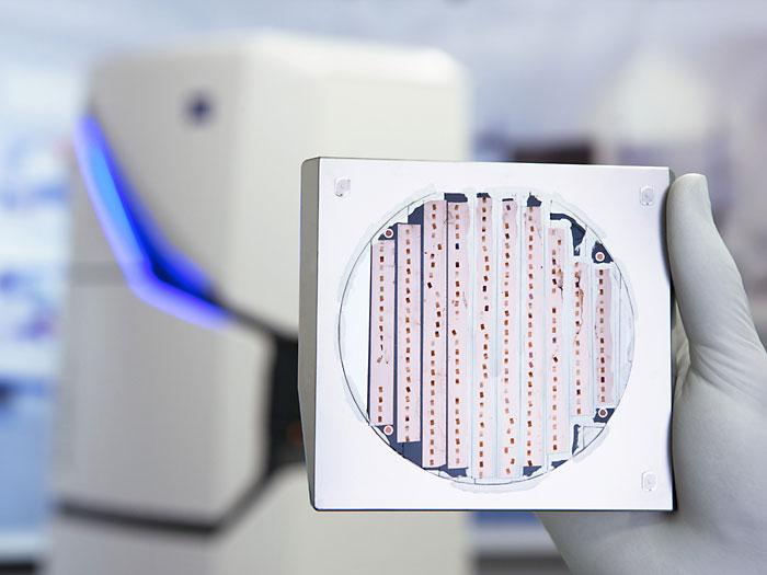
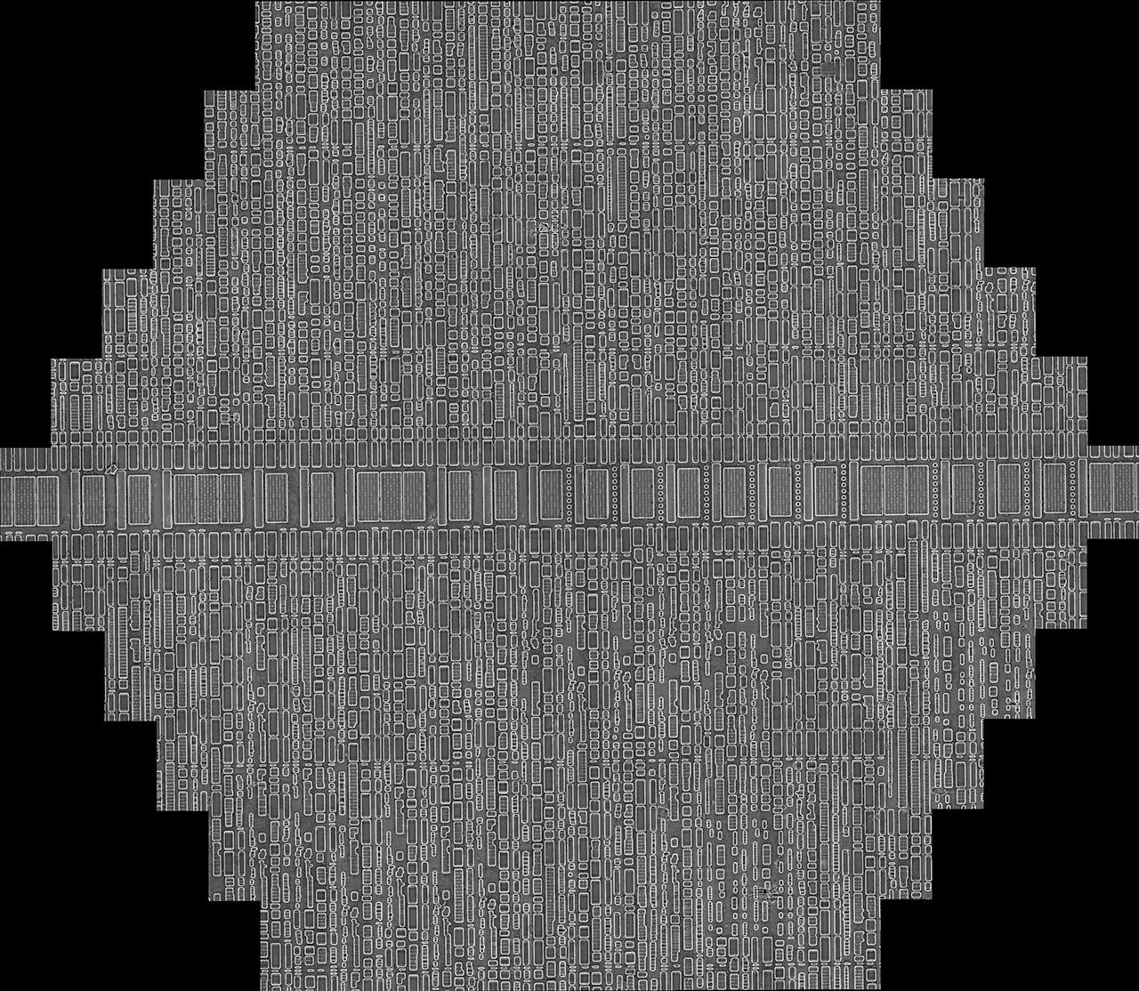
At NanoWorldMaps, advanced imaging tools like mSEMs are more than microscopes—they are the sensory organs of Artificial Intelligence. These instruments generate petabyte-scale, nanometer-accurate data that allow AI not just to analyze, but to perceive the complexity of the physical world.
Whether mapping brain connectivity in neuroscience, revealing hidden structures in materials, or inspecting semiconductor architectures, this data is the foundation for deep scientific insight. Precision imaging enables precision thinking—empowering AI to support research at a new level of clarity and scale.
