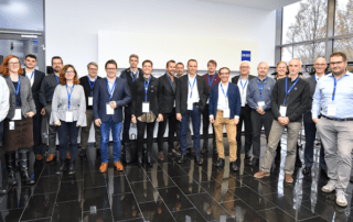
Additional consortium partners sign ‚Memorandum of Understanding‘
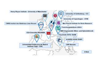
Additional consortium partners sign 'Memorandum of Understanding' for NanoWorldMaps Research Infrastructure We are delighted that several additional consortium members have chosen to sign the NanoWorldMaps 'Memorandum of Understanding' and we welcome our most [...]
Memorandum of Understanding now in effect for NanoWorldMaps
Memorandum of Understanding now in effect for NanoWorldMaps Following on from the Letters of Intent submitted by interested parties in 2019, which helped to make clear the likely applications for very high throughput electron [...]
2nd annual meeting of the NanoWorldMaps consortium 2020
2nd annual meeting of the NanoWorldMaps consortium 2020 A half-day online meeting of the NanoWorldMaps consortium was held on 4th November 2020 in order to exchange scientific experience with large-area high-speed and high-resolution imaging, [...]
Design study favourably reviewed, but not funded
Design study proposal In late 2019, the NanoworldMaps consortium submitted a proposal for an EU funded infrastructure design study (call H2020-INFRADEV-2019-3). The concept involved an international network of several multiple-beam scanning electron microscope [...]
1st annual meeting of the NanoWorldMaps consortium 2019
1st annual meeting of the NanoWorldMaps consortium 2019 In October 2019, a number of European imaging scientists met on the premises of Carl Zeiss Microscopy in Oberkochen (Germany) to discuss the possible applications [...]
